
The emerging field of biointerfaces, as interacting regions between technology and life, requires innovative design and manufacturing strategies, to develop and use their remarkable potentials, especially with regard to the engineering of biomedical appliances. Within the human body, miniaturized medical devices with hierarchical or multi-scale biointerfaces, capable of interacting at cellular, organic, and systemic levels, may perform in more biocompatible ways and even help to control the fate of cells and tissues. In vitro testing devices and surgical tools may also benefit from design-controlled biointerfaces, to achieve more controlled interactions during their missions. This article summarizes a long-term collaboration between research groups from the Karlsruhe Institute of Technology (KIT) and from the Technical University of
Madrid (UPM) in the field of biointerfaces for medical engineering applications. Synergies between the working groups have led to innovative approaches for the design and fabrication of functional textures, which are reviewed.
Der stetig zunehmende Einsatz biologischer Grenzflächen, mehr und mehr als Interaktion zwischen Technologie und Leben, erfordert innovative Design- und Fertigungsstrategien, um ihre Potentiale weiter zu entwickeln und zu nutzen, insbesondere im Hinblick auf die Entwicklung von biomedizinischen Geräten. Innerhalb des menschlichen Körpers müssen miniaturisierte medizinische Systeme mit hierarchischen oder multiskaligen Biogrenzflächen, die auf zellulärer, organischer und systemischer Ebene miteinander interagieren, verstärkt biokompatibel funktionieren und können dann sogar dazu beitragen, das Verhalten von Zellen und Geweben zu kontrollieren. Auch In-vitro-Testgeräte und chirurgische Instrumente können von design-kontrollierten Biogrenzflächen profitieren, zum Beispiel um während ihres Einsatzes gezielte Interaktionen zu ermöglichen. Der vorliegende Beitrag fasst eine langfristige Zusammenarbeit zwischen Forschungsgruppen des Karlsruher Instituts für Technologie (KIT) und der Technischen Universität Madrid (UPM) auf dem Gebiet der Biogrenzflächen für medizintechnische Anwendungen zusammen. Die Synergien zwischen den Arbeitsgruppen haben zu innovativen Ansätzen für das Design und die Herstellung funktioneller Oberflächen im Bereich der Medizintechnik geführt.
1 Introduction
Surface topographies or textures radically affect the properties and performance of materials and devices; consequently, important research efforts are being targeted at the discovery and mastering of innovative texture design and production processes. Optical properties like colour, reflectivity and overall aesthetic aspect of materials and components can be fine-tuned by modifying surface texture. Tribological contact phenomena like adhesion, lubrication ability and wettability, linked to the development of self-cleaning objects, can be also controlled through texturing. Even the ergonomics of devices or the flavour of processed food can be importantly improved through texturing strategies.
Adequately controlling the surface textures of materials and devices and straightforwardly achieving an affordable mass-production is necessary, in order to promote the societal impact of the several types of devices that may benefit from counting with functional surfaces for enhanced interactions with their environment. These functional surfaces will promote the sensory and actuation abilities of engineering products, will help to interact in a more efficient way with microorganisms for better understanding and dealing with disease, will enhance the sustainability and durability of energy conversion processes or appliances and will break down the frontiers between natural and synthetic systems, between biology and engineering [1].
To this end, research groups from the Karlsruhe Institute of Technology (KIT) and the Technical University of Madrid (UPM) have been collaborating, for more than six years now, exploring processes for designing and prototyping devices with functional surfaces and defining manufacturing chains, to achieve tools with surface microstructures and mass-produced polymeric components with controlled textures. These studies [2–10] have been performed with the continued support of the Karlsruhe Nano Micro Facility (KNMF) at KIT (www.knmf.kit.edu), a Helmholtz Research Infrastructure.
Some of the studied approaches to designing and producing such textures are detailed described in the following sections; directions for application and future research are discussed towards the end of the article.
2 Designing of functional textures
Different approaches coexist for the design of textured materials, components and devices, most of them relying on computational modelling tools. Perhaps the most direct one is based on the application of state-of-the-art CAD (computer-aided design) resources for generating patterns by using arrays of micro-(holes, columns, bumps), normally combining solid design operations, matrix-based tools and Boolean operations. Specific design software or CAD modules have been also developed, like Materialise 3-matic or Hypermesh Optistruct, to enable topology and topography optimization processes, as well as the mapping of 2D images, whose variations of colour or shade are used to create textures upon complex 3D surfaces.
Another option relies on the employment of mathematical functions, which are able to define infinite multi-scale surfaces (even in a single line of code) and to store them in the form of surface matrices, which can be further processed or linked to computer-aided manufacturing systems. These math-based surfaces can be also hybridised with the surface matrices generated from the CAD files of previously designed objects, to apply functional regions to desired portions of an object.
The different approaches differ in terms of use of computational resources, design versatility, control upon final results, adequacy for reaching hierarchical or multi-scale structures and software cost. For example, the conventional CAD-based approach rapidly leads to large sized files, which are difficult to process, in spite of its very direct applicability. The use of specific CAD complements for controlling topography is a nice option for texturing complex surfaces using collections of images, although these resources are normally expensive. The math-based approach requires from programming skills, but is unbeatable in terms of defining multi-scale surfaces, for instance by using recursive functions and fractal models, which are also very well suited for imitating nature and the extremely interesting features and functions of natural materials and living organisms. Combining these strategies promotes design versatility.

Fig. 1: Examples of hierarchical functional surfaces achieved by combining CAD-based arrays of regular and wavy features with math-based bioinspired fractal textures: bridging the gap between micro and nano systems by design
Figure 1 presents some examples of hierarchical (or multi-scale) functional surfaces achieved by combining CAD-based arrays of pillars and pyramids:
- with math-based bioinspired fractal texture,
- with the intention of controlling the wettability properties of surfaces and devices,
- with promoting anti-fouling and self-cleaning effects for enhanced performance (i. e. self-cleaning surgical tools for remote regions, implants with improved compatible response, and smart diagnostic systems).
3 Producing of functional textures
In many cases, the surface texture of objects is just a consequence of the materials and technologies employed for their manufacture. Several physical-chemical processes are able to synthesise or process materials with porous structures and textured surfaces. Both top-down (i. e. chemical etching, laser ablation) and bottom-up (i. e. molecular self-assembly, chemical and physical vapour deposition) alternatives can be found in the technological portfolio. However, to achieve better design-controlled microstructures, especially in connection with final polymeric components, alternative manufacturing chains, capable of transforming design files into real products are needed.
Different additive manufacturing technologies (AMTs), from fused-deposition modelling and digital light processing, to selective laser sintering and powder-based laser fusion, have proven very useful in the last decades and somehow transformed traditional approaches to product design and engineering. These additive resources, which normally work on a layer-by-layer fashion, help to rapidly obtain both prototypes and final parts using many different materials, including: metals, polymers, ceramics, composites and even from biological origins. They prove especially useful when dealing with very complex geometries, due to the fact that the additive processes enable a sort of solid freeform fabrication.
Nevertheless, most AMTs are not yet competitive with traditional mass-production processes. Besides, as regards a precise control of surface topography, the layer-by-layer construction normally leads to visible lines of material. In other cases, the sintered powders can be appreciated, with final components having a sort of granular aspect. Again, in most cases surface texture is a consequence of processing and can not be adequately managed towards functional surfaces with specific purposes, for which post-processes are normally required.
To solve these issues, the collaboration of partners within KNMF has successfully integrated different materials and technologies with multi-scale ambition and achieved metallic and polymeric components with surface microstructures controlled from the design stage. Topographic details of less than 10 mm3 have been achieved and helped to functionalise the surfaces of different mass-produced microsystems over areas of several square centimeters, hence showing potential for a wide set of industrial applications. The manufacturing chain, with its alternatives, is detailed below.
First of all, the designed microstructured surface or textured object is created, as a master model, using direct laser writing, an additive manufacturing technology based on the two-photon polymerization of photo-resins and currently the most precise technology from the additive realm. The system employed in the studies, carried out by the authors, is the Photonic Professional tool from Nanoscribe GmbH (www.nanosribe.com), a spin-off from Karlsruhe Institute of Technology. After obtaining the master model in polymeric resin on glass or silicon substrate and performing a coating (Cr and Au) for making the surface conductive, a special nickel electroforming process is performed. This thick galvanic nickel deposition process leads to surface microstructured metal blocks, which can be used either as mass-production tools (mould insert or shim) or as final metallic parts with functional surfaces.
In some cases, an additional processing by laser ablation may help to further process the metallic part for different purposes, like
- the generation of channels for microfluidic systems,
- the elimination of some textures for generating selective transitions of textures or
- the creation of interlocking elements, if additional interactions with other components are foreseen (all this as a complement to features defined in the original CAD models).
Final mass-production of polymeric microstructured devices can be obtained by incorporating the electroformed surface structured metallic tool into the mould frameworks of injection or compression moulding, as well as hot embossing machines, in which the mass-processing of thermoplastics is possible.
Figures 2 and 3 present some examples of the results from design-controlled fabrication of functional textures in polymers and metals. Images from figure 2a present a couple of math-based designs of bioinspired hierarchical textures, while images from figure 2b show the details of two direct laser written surfaces, which can be used as master models for the creation of mass-production tools by thick galvanic nickel deposition, as previously explained. Besides, the textures can be applied to desired regions of a surface, to define design-controlled gradients of textures, hydrophobic/hydrophilic transitions, microchannels and microwell surrounded by textures, microtextured spots for trapping cells and microorganisms, among others.

Fig. 2: Design-controlled fabrication of functional textures, done by a Design model (a), and shown as SEM images from direct laser written master models made in polymeric resist material (b) and SEM images from structures replicated (using nickel mould inserts; see fig. 3) in PMMA by hot embossing at 165 °C (c)

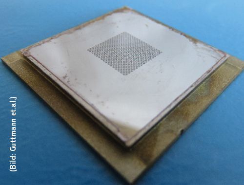
Fig. 3: Fabricated mould insert in nickel (using electroforming) for the replication of functional hierarchical textures; a) picture of the full insert (a) and SEM images of the structures in nickel (b), which are inverse to the laser-written resist structures (fig. 2b)
Figure 2c shows, as example, images of the final hot-embossed components, in this case showing an arrangement of hierarchical bumps forming a vascular-like branched network for cell culture purposes [7–10].
Figure 3 shows some details for the galvanic replication (made by nickel electroforming) of the laser-written resist structures. It is important to point out that the combination of high-precision additive manufacturing with electroforming leads to unprecedented level of detail and complexity in metallic parts and tools for injection moulding and hot embossing of thermoplastics.
4 Applications for functional textures
Industrial applications of the described design and production processes for functional surfaces are extremely varied but the connection to the increasingly relevant field of biointerfaces is of special importance. According to Wikipedia [11], biointerfaces can be defined as the regions of contact between biomolecules, cells, biological tissues or living organisms or organic materials considered living with another biomaterial or inorganic/organic material. Biointerfaces are essential for the biological integration of implants and for their long-term viability, for a wide set of biological micro-electro-mechanical-systems (Bio-MEMS) used for studying disease, and for the development of biohybrid living machines, to cite just some of their remarkable potentials [1].
Among different proposals for various applications already validated during the collaboration between KIT and UPM, the authors would like to put forward:
- a collection of prototypes of bio-MEMS designed for controlling cell populations on lab- & organ-on-a-chip systems,
- a set of surfaces with hydrophobic/hydrophilic transitions with application for innovative microfluidic systems capable of controlling fluids by gradients of wettability and with potentials towards self-cleaning surgical tools or
- implants with enhanced biocompatibility, more rapid osseointegration or even smart responses to human body conditions along the healing process.
These types of devices [6, 10] have already proven useful for positioning cells to desired positions of biomedical microdevices used for modelling disease. The control of cell populations on cell culture systems and organ-on-a-chip platforms, fixing them to desired positions, enables the creation of biomimetic, physiological-like environments for better recapitulating the morphology of human tissues, than when using conventional cell culture Petri dishes. The transitions of hydrophilic/hydrophobic regions can help to co-culture different cell types, requiring varied growing conditions, which is challenging. Besides, the use of microtextures forming geometrical patterns supports cell cultures adopting desired complex shapes, like needed for the creation of in vitro vasculatures with fractal-like forms. Connections with molecular nanopatterning techniques [10], with which supporting molecules for enhanced long-term adhesion or growth factors for helping to differentiate mesenchymal stem cells into different tissues can be applied, is also opening new horizons, for studying diseases like cancer and systematically assessing therapies, even in personalized ways.
Figure 4 presents another example of some of the biomedical microsystems achieved with the described combination of technologies, including:
- cell culture system with microtextured channels and variations of topography for studying their effects on cell movement and behavior [2] and
- organ-on-a-chip platform with microchannels for studying cell interactions and metastatic processes [8].
The different chambers are conceived for co-culturing different cell types conforming parenchymal tissues, like the functional tissues of brain, liver, kidneys or gut, while the microchannels represent the vasculature and the microwells can be employed for placing tumoral spheroids and exploring invasive processes. Thanks to the straightforward mass-production of these sorts of microsystems, multiplexation and systematic testing is promoted.

Fig. 4: Cell culture system (a) with microtextured channels for studying the effects of surface topography on cell movement (and detailed view of a microtextured channel); moulding tool for the mass-production of organ-on-a-chip devices and replicated part in PMMA (b) and cell interactions across microchannels studied (c) using a mass-produced organ-on-a-chip microsystem (courtesy of Prof. Josefa Predestinación García-Ruíz; additional details in [2, 8]
5 Textures towards the future
Current challenges to achieve complex engineering devices with functional textures are linked to increasing the scale-range, upon which these processes can be applied. Achieving details of less than 1 mm3 over areas of around 1 m2 would be a remarkable breakthrough. Increasing the materials families that can be functionalized through similar design and production chains, from the already validated polymers and metals, to innovative areas linked to ceramics, composites and biological materials, is another key issue.
These advances would undoubtedly help to expand the applications of functional textures, from the already studied and validated concepts in the bio-MEMS and metamaterials fields, towards
- human implants with enhanced biointegration for the biomedical industry,
- car bodies with self-cleaning properties or with enhanced aerodynamics for the transport industry,
- special anti-fouling transparent surfaces for solar cells with extended life and
- even smart energy-efficient facades for architecture.
International and multidisciplinary research collaborations, through open research infrastructures like the KNMF at KIT, will for sure be a clue for bringing these revolutionary concepts to life.
Acknowledgements
This work has been carried out within a variety of different projects including a high financial and personal support of the Karlsruhe Nano and Micro Facility (KNMF), a research infrastructure of the Helmholtz-Community at the Karlsruhe Institute of Technology (KIT). The authors, especially Andrés Díaz Lantada, would like to thank for the excellent support by all the involved colleagues from the Institute for Microstructure Technology, the Institute of Applied Materials and the KNMF user office at KIT (see: www.knmf.kit.edu).
References
[1] C. Niemeyer, M. Bastmeyer, S. Bräse, J. Lahann, C. Wöll: White paper on the biologization of materials research; Preprints, December 17 (2018); doi:10.31219/osf.io/7wqm9
[2] S. Hengsbach, A. Díaz Lantada: Rapid prototyping of multi-scale biomedical microdevices by combining additive manufacturing technologies; Biomedical Microdevices, 16 (2014) 617–627; doi:10.1007/s10544-014-9864-2
[3] S. Hengsbach, A. Díaz Lantada: Direct laser writing of fractal surfaces: Strategy to design and manufacture textured materials; Advanced engineering materials, 17 (2015), 172–180; doi:10.1002/adem.201400082
[4] A. Díaz Lantada, M. Guttmann, V. Piotter, K. Plewa, N. Barié, M. Wissmann: Towards mass production of microtextured microdevices: linking rapid prototyping with microinjection molding; Int. J. Adv. Manuf. Technol., 76 (2015) 1011-1020; doi: 10.1007/s00170-014-6333-2
[5] A. Díaz Lantada, A. Muslija, J. P. Garcia-Ruiz: Auxetic tissue engineering scaffolds with nanometric features and resonances in the megahertz range; Smart Materials and Structures, 24 (2015) 055013/1–14; doi:10.1088/0964-1726/24/5/055013
[6] A. Díaz Lantada, G. Begasse, A. Morss Clyne, S. Hengsbach, M. Guttmann, V. Piotter, K. Plewa, P. Smyrek, M. Pfleging: Towards reliable organ-on-chips and humans-on-chips; A. Díaz Lantada (ed.), Microsystems for Enhanced Control of Cell Behavior, Studies in Mechanobiology, Tissue Engineering and Biomaterials 18, (2016) 389-408; doi: 10.1007/978-3-319-29328-8_22
[7] A. Díaz Lantada, S. Hengsbach, K. Bade: Lotus-on-chip: computer-aided design and 3D direct laser writing of bioinspired surfaces for controlling the wettability of materials and devices; Bioinspiration & Biomimetics, 12 (2017) 066004; doi:10.1088/1748-3190/aa82e0
[8] A. Díaz Lantada, W. Pfleging, H. Besser, P. Smyrek, M. Guttmann, M. Wissmann, V. Piotter, K. Plewa, J.P. García-Ruíz: Research on the methods for the mass production of multi-scale organs-on-chips; Polymers, 10 (2018) 1238; doi: 10.3390/polym10111238
[9] A. Díaz Lantada, R. Kumar, M. Guttmann, M. Wissmann, M. Schneider, M. Worgull, S. Hengsbach, F. Rupp, K. Bade, M. Hirtz, S. Sekula-Neuner: Synergies between surface microstructuring and molecular nanopatterning for controlling cell populations on polymeric biointerfaces; Polymers, 12(3) (2020) 655; doi: 10.3390/polym12030655
[10] A. Díaz Lantada, N. Mazarío Picazo, M. Guttmann, M. Wissmann, M. Schneider, M. Worgull, S. Hengsbach, F. Rupp; K. Bade, G. R. Plaza Baonza: Soft-lithography of polyacrylamide hydrogels using microstructured templates: Towards controlled cell populations on biointerfaces; Materials, 13 (2020) 1586; doi:10.3390/ma13071586
[11] Wikipedia; Article on Biointerfaces; accessed on July 15th, 2020
DOI: 10.7395/2020/Guttmann3
1 Universidad Politécnica de Madrid (UPM); Mechanical Engineering Department; c/José Gutiérrez Abascal 2,
ES-28003 Madrid, Spain
2 Karlsruhe Institute for Technology (KIT); Institute for Microstructure Technology (IMT); Hermann-von-Helmholtz-Platz 1, D-76344 Eggenstein-Leopoldshafen, Germany
* E-Mail: andres.diaz@upm.es
# E-Mail: markus.guttmann@kit.edu
