INM among the 21 German exhibitors at nano tech 2014 in Japan

The INM – Leibniz Institute for New Materials will be presenting its latest developments at this international trade fair for nano materials. In doing so, it will strengthen its international focus and strategic partnership with Japan. From 29 to 31 January, it will be in the German Pavilion where it will showcase its expertise in nanotechnology-based coatings with special properties. These include antimicrobial coatings, transparent and conductive layers, the printing of electronic conductor tracks on a micrometre and nanometre scale or coatings, which enhance the efficiency of solar cells. The INM will also explain developments in which adhesion on surfaces can be switched on and off.
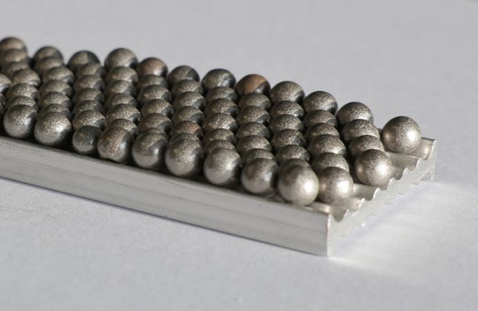
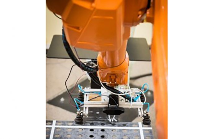
Switchable adhesion principle for non-residue gripping in a vacuum – Automotive, semiconductor and display technologies as well as manufacturers of complicated lens systems use components with highly sensitive surfaces for their products. During the production process, such parts are transported back and forth in many process steps. Each process of lifting up and lowering using conventional gripping systems carries the risk of residues adhering or damage being caused to such surfaces. Sucker systems reduce residues, but they do not work in a vacuum. The researchers at the INM have now advanced the gecko adhesion principle to such an extent that they are now also able to switch it on and off in a vacuum.
Glass-like diffusion barrier for flexible CIGS solar cells for spraying – Researchers at the INM have developed a barrier layer for flexible CIGS solar cells which separates the metal substrate from the absorber layer and so increases the efficiency of the metal-based solar cells. A wet chemistry spray process can then be used to apply it to flexible and rigid substrates with a variety of shapes.
Printed transparent conducting oxide layers on film – TCOs are normally produced on solid substrates using vacuum coating such as sputtering, but can also be applied to flexible substrates such as plastic film using special TCO inks. To do this, developers at the INM use TCO inks containing TCO nanoparticles and produced using wet chemistry processes. This method enables not only application to plastics and films but also, for the first time, direct printing of transparent conductor structures.
Photometallization: Different size electronic strip conductors in the one-step process – Electronic conductor strips determine the operational capability of a number of devices and instruments such as in TFT screens on displays and touch screens or in transponders in RFID systems where structures with large conductor strips measuring several millimeters vary, the smallest structures measuring just a few micro- or nanometers. Up to now, these conductor strips have been manufactured in different production stages, but researchers at the INM have developed a new process with which they can create macroscopic and microscopic conductor strips in a single production step
Anti-microbial coatings with a long-term action – Hygienic conditions and sterile procedures are particularly important in hospitals, kitchens and sanitary facilities, air conditioning and ventilation systems, in food preparation and in the manufacture of packaging material. In these areas, bacteria and fungi compromise the health of both consumers and patients. Researchers at the INM have now produced antimicrobial coatings with both silver and copper colloids with a long-term effect that kill germs reliably and at the same time prevent germs becoming established.
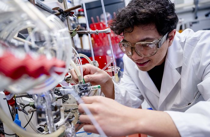
INM conducts research and development to create new materials – for today, tomorrow and beyond. Chemists, physicists, biologists, materials scientists and engineers team up to focus on these essential questions: Which material properties are new, how can they be investigated and how can they be tailored for industrial applications in the future? Four research thrusts determine the current developments at INM: New materials for energy application, new concepts for implant surfaces, new surfaces for tribological applications and nanosafety/nanobio interaction. Research at INM is performed in three fields: Chemical Nanotechnology, Interface Materials, and Materials in Biology.
INM – Leibniz Institute for New Materials, situated in Saarbruecken, is an internationally leading centre for materials research. It is an institute of the Leibniz Association and has about 190 employees.
www.inm-gmbh.de
Aktuelle Onlineartikel
-
29. 01. 2025 Fraunhofer-Forschende entwickeln einzigartige Dämpfung für Werkzeugmaschinen
-

29. 01. 2025 Tarnkappe nach Chamäleon-Vorbild entwickelt
-
29. 01. 2025 Robotik und Automation drehen ins Minus
-
22. 01. 2025 Upcycling weist den Weg zur Wirtschaftlichkeit
-

21. 01. 2025 KI-gestützte Datenanalyse deckt Probleme in wissenschaftlichen Publikationen auf
-
20. 01. 2025 Wie man Kohlenstoffdioxid aus Abgasen recyclen kann